
Wafer Metrology and Inspection - additional quality steps
Dicing-Grinding Service utilizes detailed examination of the product’s pre- and post-process condition. Advanced metrology and AOI are part of the daily production. Several challenges may occur e.g. when processing advanced packaging products: eWLB, WLCSP, TSV, Bumping or Flip-Chip are the keywords. Advanced metrology and AOI are supporting us at conquering those challenges as well as developing and evaluation of new processes such as laser dicing or ultra thin grinding.
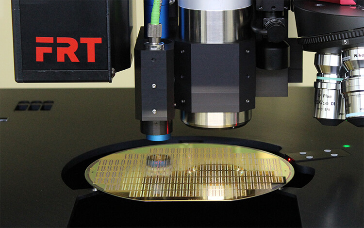
Metrology
Our 3D surface metrology system consisting of an IR/White Light enables the measurement of waferstacks, compound material thickness, warpage, surface deviations, bump height and a lot more features. Measuring surface roughness can be achieved with Atomic Force Microscopy (AFM). Advanced metrology is performed with MicroProf® tools from our strategic partner FRT.

Automated Optical Inspection (AOI)
Profitability, security and reliability of products are vital. To enable that, AOI shifts into focus. AOI can be used for several applications like chipping/crack detection or wafer bumps. Advanced optics, 2D/3D options and comprehensive software enable various possibilities of defect detection applicable to any IC based structure. For AOI services we utilize the Eagle and Condor products from our strategic partner Camtek.
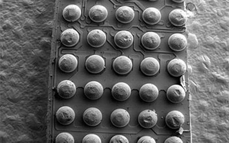
Scanning Electron Microscopy (SEM)
The scanning electron microscope SEM can be perfectly utilized for semiconductor manufacturing and processing. The properties of semiconductor structure can be inspected very well due to the various contrast modes and super high resolution. That’s why we are using SEM in our new cleanroom for the Dicing-Grinding Service. Utilizing SEM, material characterization and quality assurance can be accomplished holistically: SEM in combination with AOI and AFM.
Send us your service request now
Contact us